SEMICONDUCTOR
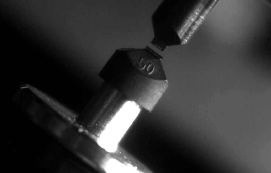
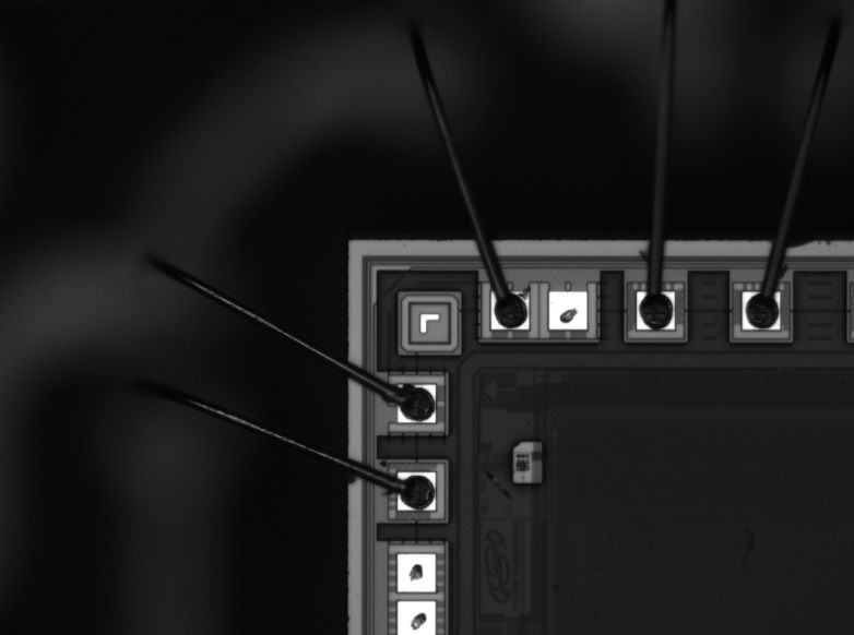
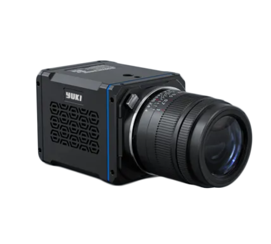
In the semiconductor manufacturing process, a high-speed camera like a YUKI camera is commonly used for optical inspection, allowing detailed analysis of critical features on wafers by capturing rapid changes during the manufacturing process, including identifying defects, measuring dimensions, and observing the behavior of materials during specific steps like etching or deposition; essentially providing a visual analysis of the microscopic world on the wafer surface at high frame rates.
Key points about using high-speed cameras in semiconductor manufacturing:
- Detailed defect detection:
High frame rates enable the capture of subtle variations in the wafer surface, allowing for precise identification of even minute defects that might be missed with standard inspection methods.
- Process monitoring:
By capturing rapid changes during manufacturing steps, engineers can analyze and optimize process parameters like deposition rates or etching uniformity.
- Failure analysis:
High-speed cameras can be used to capture the moment of failure during stress tests, helping to identify potential weaknesses in the design or manufacturing process.
- Alignment and precision:
Precise synchronization with the wafer movement allows for accurate capture of specific features on the wafer.